


Have a specialist call me
Leave your details and we will contact you personally.
Something went wrong, please try again.
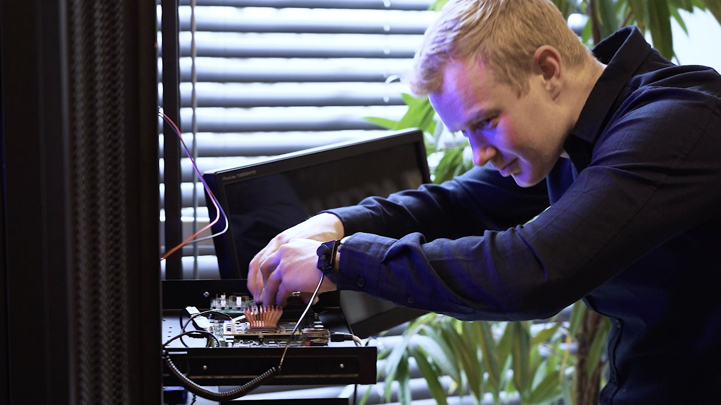
It is common practice to let dedicated board developer’s layout printed circuit boards (PCBs). However, more and more often the PCBs do not meet their design goals during the testing phase. Why is that? And what is the solution? The answer lies in the complexity of its design, the applied technology, and the correct tools.
Until recently, it was a regular job to have board developers design PCBs. The design rules were clear and the results generally predictable. However, over the recent years, PCBs are resulting in unpredictable behaviors, with painstakingly long problem-searching endeavors to find the root causes. The root cause of the failures: current PCBs regularly are required to pass the multi-Gigahertz signaling threshold, and with that, it has become extremely hard to detect failures after production.
Why is it difficult to detect failures?
Passing the Gigahertz frequency boundary means that PCB technology becomes complicated, component densities go up as well as the power consumption. ‘The board starts to behave like an analog component instead of a digital one’, says Dirk van den Heuvel, product manager at TOPIC. ‘It requires knowledge and skills of analog circuit design, which is rare to find in this digital era. Hence why the bare boards fail more and more often and understanding or measuring the root causes is more complicated than ever.’
Extreme or common practice?
An illustrative example is the exa-scale computing processor blade (CRDB), TOPIC recently developed for the EuroEXA.eu project. This board contains a high-end Xilinx FPGA as well as a SOC, 4x DDR4 memory banks, 4x 100Gbps communication links and a COM-Express interface. This resulted in a 30-layer PCB with buried, blind, micro, and thermal via’s; having to transport around 200A of current at 0.85V. To reach the intended compute performance of 1018 instructions per second, 150.000 of these blades are foreseen in the system, leading to a power need of over 20MW. Although this sounds massive, it is still only 20pW per instruction where an i7-based PC requires around 500pW per instruction.
Measuring interaction
These more advanced boards require pre-solving the potential problems during the design phase. Applying PCB simulation-based strategies like signal integrity, power integrity and thermodynamic analyses help discover potential design flaws and complicated interactions. ‘This way, we can see how the various elements on a board interact physically and we influence their behavior when needed.’ E.g., the thermal simulation of the board layout of the processor blade board revealed impedance variations due to via’s penetrating the power planes. This leads to thermal losses and non-uniform distribution of supply voltages. And every 1% power loss translates into 200kW energy loss in the whole system! Given the sustainability goals, this is not at all desirable.
Therefore, it is wise to design, simulate and test the PCB properly and on time. ‘Once in production, it is near impossible to fix these issues’, says Van den Heuvel. ‘Considering the manufacturing cost of PCBs, project timeline delays, scarcity of materials as well as the long term impact to the planet, it is much better to have as little failure as possible.’
Do you have any questions or would you like to know more?
Contact us without obligation.
We are happy to help you personally.
Leave your details and we will contact you personally.
We will contact you by telephone shortly.
Leave your details and we will contact you without obligation.
We will contact you by e-mail shortly.